>


Limitations with Semiconductor Plastic Packages


July 2022


  • Decades ago the overwhelming majority of commercial semiconductors were packaged in ceramic packages. High temperature downhole tools as well as Aerospace and Military hardware benefited from these ceramic packages due to their ability to withstand and dissipate high temperatures. As time and materials technology progressed, semiconductor manufacturers, in their efforts to reduce costs, migrated to various types of plastics to encapsulate the component die and leadframes (component body). Initially, with regards to the hostile environment applications, plastics were a dismal failure. Texas Microelectronics was witness to this. Many companies required their engineers and buyers to exclusively utilize ceramic parts in their products. As plastic technologies progressed, so did the reliability and high temperature survivability of these components. By the time we reached the 2000’s, more closely to the 2010+ timeframe, plastic component technology had progressed to the point where companies began to use these parts at temperatures ranging from 150 to 175°C, and in some cases briefly up to 200°C.


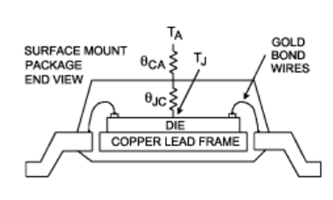
  • So, what are the limitations with plastic components? Lifespan and reliability. Despite the advances in plastic component bodies/encapsulation, with regards to hostile environment and or high-performance applications, there are limitations in the use of plastic components. Further to the point, the problem of CTE mismatches (Coefficient of Thermal Expansion) between differing materials comes into play. Thermal resistance of the component body material is critical. As the internal die self-generates heat, that heat must dissipate out into, and then out of, the plastic encapsulation material. Plastic is not a good conductor of heat, so that dissipation factor would be considered to be “poor”. Compounding this issue is the CTE mismatch between the silicon die, the wire bonds, and the plastic component body material. The heat dissipated by the die must travel through the plastic material, then from the plastic to free air in the outside world. When these CTE mismatches reach a certain level, the ability of the different materials to expand and contract equally is exceeded. The primary and typical first failure mode is a disconnection (by shearing effect) of the wire bonds from the die pads, and hence component failure.


  •  
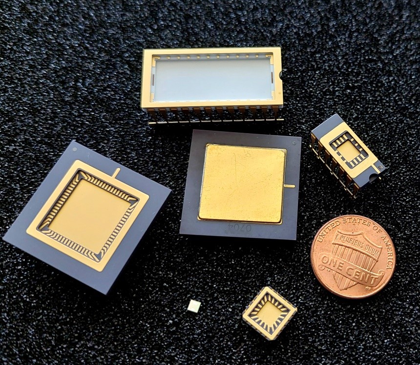
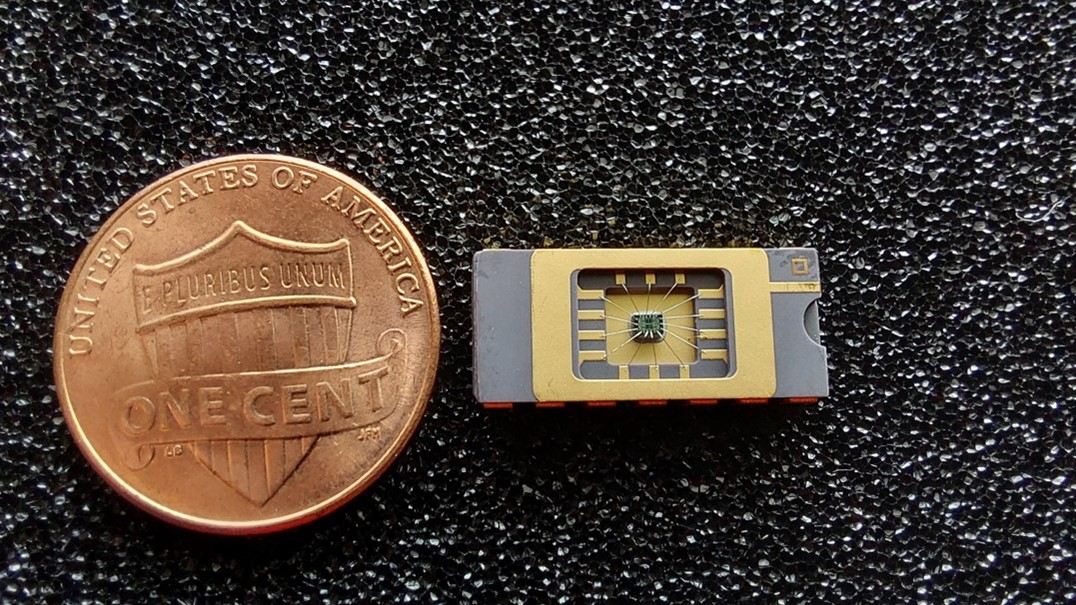
  • Here’s where ceramic or Kovar (metal) packages outperform any plastic packaged part. Ceramic and Kovar are excellent conductors of heat. The inside of a ceramic or Kovar package contains a cavity where a single die, or multiple in the case of a true Hybrid, is placed. After die placement and the wire bonding process, there is no encapsulation material touching the die, or the wire bonds. The product cavity is sealed in (typically) 100% gaseous Nitrogen, which prevents any oxidation within the component, and eliminates the CTE issues created by plastic materials. The absence of the plastic material surrounding the die and wire bonds enables this device to operate at much higher temperatures, and for a much longer timeframe.


    • Monolithic die re-packaged in Ceramic 

    •  
    • The initial higher cost of a ceramic component or hybrid is easily justified when considering device lifespan and superior performance. If your company truly wants to excel in the high-performance, hostile-environment markets, then ceramic or Kovar components are the right choice. Texas Microelectronics can get you there.


    6 Top Benefits of Hybrid Microelectronic Technology


    June 2022


    • High Temperature Operation: The absence of plastic packaging used in traditional semiconductors allows hybrid microelectronic components to operate at much higher temperature ranges (175-200C+).  Hybrids, with a Nitrogen filled die cavity, do not suffer the CTE (coefficient of thermal expansion) mismatches that plastic components do.  Mechanical CTE mismatches are one of the leading causes of wire bond failures in plastic packaged semiconductors, when operating at very low or very high temperature ranges.  Wire Bonds in Hybrid Microelectronics are not potted in encapsulation material.  They are free standing in inert gaseous Nitrogen.
    •  
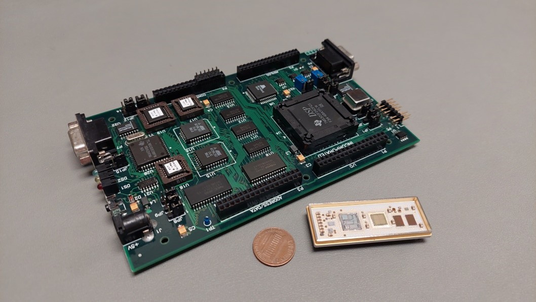
    • Real-estate footprint reduction:  For any given circuit migrated to Hybrid technology, the absence of plastic packages with SMT and or PTH components, discrete wires, a printed circuit board, and connection cables, the real estate savings are significant to say the least.  Migrating from a traditional PCBA to a Hybrid circuit can reduce the necessary footprint by as much as 10-20X.
    •  


    • Circuit Longevity:  With regards to operation in a high temperature environment, 185-225°C, the absence of traditional component solder, even with the usage of HMP solder (High Melting Point), Hybrid Technology can greatly extend the life cycle of the circuit.  Hybrid technology can completely eliminate component solder from the assembly equation.  So, what’s the issue with solder at these extreme high temperature ranges? Electrochemical Metal Migration.  Greatly simplified, this EM Migration is a phenomenon that under the action of high-density current, exacerbated by high temperatures, atoms or ions migrate with electrons, leading to the component segregation in solder joints.  The metals in the solder actually migrate from one area to another, creating a failed connection point.  Our experience regarding circuit life, when comparing a Polyimide Printed Circuit Board to Hybrid Technology, is that Hybrid circuits have an operating life 6-10X greater than the Printed Circuit Board.  We regularly have clients that remove our Hybrids from “old” machinery or tools (planned product lifecycle), retest the Hybrids, then install them in a new tool or machine set.  The relatively high initial cost of Hybrids is greatly justified.
    •  
    • Electrical Performance: In a manner of speaking we’re back to real estate (size).  The very small physical geometries of a Hybrid substrate, and the very short distances between each piece of silicon semiconductor and passive components (measured in thousandths of an inch) lend to exceptional electrical performance of the circuit, including but not Iimited to: reduced noise levels, increased signal speeds, and superior thermal management.
    •  
    • Mechanical Durability: Put simply, Hybrid circuitry is placed in a ceramic or metal package, then hermetically sealed (a type of weld).  It can’t be scratched or contaminated chemically or with particulates.  It can’t be bent, or flexed, or suffer delamination that Printed Circuit Boards can experience.  Hermetic technology.
    •  
    • Security: There’s plenty of talk around the world regarding technology theft and technology copying.  There are actors worldwide actively engaged in reverse-engineering technologies for the purposes of copying the product.  The reverse-engineering of a typical Printed Circuit Board circuit, while complicated and requiring a high skill level, can be done if the motivation is high enough to justify the effort and expense.  Reverse-engineering a Hybrid is a near impossible task due to the usage of raw, unmarked, silicon semiconductors and passive components.  Traditional Surface Mount Components (SMT) and Plated Through-Hole Components (PTH) are typically marked to identify the part number and a manufacturer’s date code, while raw Hybrid components are sanitized from such markings.  Your circuitry IP is safe in a Hybrid package.
    •  
    •  

    •  


      Die-Level Semiconductor Programming


      May 2022


      Field Programmable Gate Arrays (FPGA), EPROM, EEPROM, FLASH:

      Texas Microelectronics Corporation has the ability to program FPGA’s and most memory devices at the die level, before insertion into a package.


      This process provides the distinct advantage of reducing the total packaged pin count to power and I/O lines only. The die’s programming pins need not be connected to the package itself unless your design specifically requires them. FPGA and memory die can be placed in various package pin counts dependent upon die size and your I/O count requirements.


      These designs may be packaged in a monolithic configuration or incorporated with other die as part of a true microelectronic hybrid circuit. For high density and mixed signal components, die level programming, with additional support circuitry can be utilized to provide a solution without redesigning your entire product.


      Texas Microelectronics has been utilizing this technology for 2 decades, however recently we are seeing a significant increase in design requests for die programming and ASICs due to the worldwide supply chain shortages of traditional Commercial off the Shelf (COTS) semiconductors. 


      A programmed FPGA, or a dedicated ASIC can emulate other semiconductors therefore filling the supply chain gap, which enables our clients to continue to produce their products without interruption.


      The Semiconductor Shortage – The 3 Why’s


      April 2022


      “Semiconductor shortage”.  It’s a phrase that is becoming more common in our daily lives, and most of us are tired of hearing it.  Unfortunately, it’s not going away any time soon.


      As someone that comes from a semiconductor and electronics industry background, I’m going to share some insights as to the 3 main reasons for the shortage.  While the reasons are multicausal, I’ll keep things simple for brevity.


      It will come as no surprise to anyone that this sad story begins with the word, “COVID.”  Let’s take a step-by-step chronological look at how we got into this mess.


      First, when COVID first rose its ugly head, millions of people hid under their kitchen tables and wouldn’t even venture out of the house. 


      The first step in this mess is that car and truck sales plummeted.  When this happened, the Procurement departments of the automobile manufacturers both cancelled and greatly pushed out orders for everything, including semiconductors


      Simultaneously, the consumer demand for items such as Big Screen TV’s, cell phones, Surround Sound Systems, and Laptops skyrocketed.  The Procurement departments of these manufacturer’s then issued purchase orders for every semiconductor they could get their hands on. 


      And they got what they needed.


      Fast forward to the first half of 2021 when the COVID vaccine became widely available.  People rushed to get vaccinated, then slowly ventured back out and began to, yes, buy cars and trucks again.  As the demand for automobiles increased, the Procurement departments of the manufacturers began to place orders for semiconductors again, and were told, - “So sorry, you’ll have to wait at least a year or more as we’re all booked up from other consumer demands.”


      The consumer market for cell phones, TVs, and laptops, etc. consumed everything on the open market.  It was a double punch to the semiconductor shortage.  The above are the first 2 main reasons for the semiconductor shortage.


      Make no mistake, the semiconductor manufacturers are running their factories 24/7.  They are producing every device possible.  New questions logically arise such as, “Why don’t they build more factories?”, to which the answer is, - they are, but it takes years to plan and build a sophisticated multi-billion-dollar semiconductor manufacturing facility.


      Next, let’s talk about that third reason for the shortages, that has absolutely nothing to do with COVID.


      For a moment, and for the sake of this discussion, let’s pretend that COVID never happened.  Even without COVID, the overall demand for advancing technology in every market segment: automotive, appliances, consumer entertainment systems, etc. still moves froward, which automatically generates an ever-increasing demand for semiconductors.


      This is the trifecta that is causing the world-wide semiconductor shortage.  All indications point to a slow recovery.  Don’t expect to see any significant relief in the semiconductor supply chain until at least late 2023.


      OEM’s are going to have to get creative for the next couple of years until the shortages abate.  As an example, automobile manufacturers, in order to sell the number of vehicles necessary to meet their financial minimums, will have to offer vehicles with reduced technology options, or in other words, offer more models as “bare bones” editions.  Watch for it.  It’s coming.


      Here at Texas Microelectronics we’re seeing a significant increase in inquiries to develop and produce emulation devices to replace commercial semiconductors that are simply not available.  We welcome the challenge.


Engineering Innovative High Temperature Solutions

Copyright © 2016 TexasMicroelectronics.com  |  All Rights Reserved

Website Made in Texas by Soula Creative

Engineering Innovative

 High Temperature Solutions